


www.digiembedded.com
133
Memory Controller
Asynchronous page mode read
The memory controller supports asynchronous page mode read of up to four memory
transfers by updating address bits A[1] and A[0]. This feature increases the
bandwidth by using a reduced access time for the read accesses that are in page
mode. The first read access takes static wait read and
WA IT RD cycles. Subsequent
read accesses that are in page mode take static wait page and
WAITPAGE cycles. The
chip select and output enable lines are held during the burst, and only the lower two
address bits change between subsequent accesses. At the end of the burst, the chip
select and output enable lines are deasserted together.
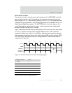
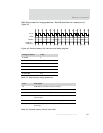
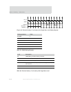
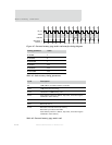
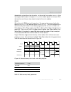
Figure 47 shows an external memory page mode read transfer with two initial wait
states and one sequential wait state. The first read requires five AHB arbitration
cycles (plus three wait states); the following (up to 3) sequential transfers have only
one AHB wait state. This gives increased performance over the equivalent nonpage
mode ROM timing (see Figure 46, "External memory 2 wait states fixed length burst
read timing diagram," on page 132). Table 61 provides the timing parameters.
Table 62 describes the transactions for Figure 47.
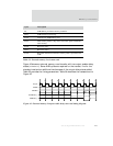
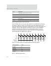
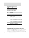
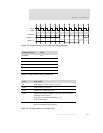
T7-T8 Read data 0 returned from the static memory.
Read data 0 is provided to the AHB.
Static memory transfer 1, address, chip select, and control signals
submitted to static memory.
T8-T9 Read wait state 1.
T9-T10 Read wait state 2.
T10-T11 Read data 1 returned from the static memory.
Read data 1 is provided to the AHB.
Static memory transfer 2, address, chip select, and control signals
submitted to static memory.
T11-T12 Read wait state 1.
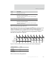
Cycle Description
Table 60: External memory 2 wait states fixed length burst read