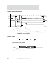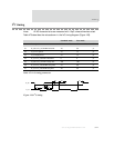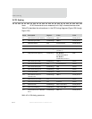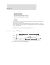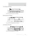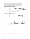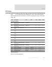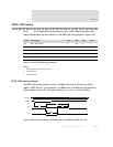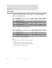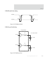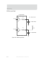
SPI timing
828
NS9750 Hardware Reference
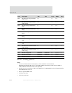
Notes:
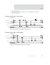
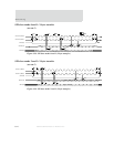
1 Active level of SPI enable is inverted (that is, 1) if the CSPOL bit in Serial Channel
B/A/C/D Control Register B is set to a 1. Note that in SPI slave mode, only a value of 0 (low enable) is
valid; the SPI slave is fixed to an active low chip select.
2 SPI data order is reversed (that is, LSB last and MSB first) if the BITORDR bit in Serial Channel B/A/C/D
Control Register B is set to a 0.
3 T
BCLK
is period of BBus clock.
4 ±5% duty cycle skew.
5 ±10% duty cycle skew.
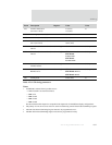
SP14 SPI enable low setup to first SPI
CLK in rising
30 ns 0, 3 1
SP15 SPI enable low setup to first SPI
CLK in falling
30 ns 1, 2 1
SP16 SPI data in setup to SPI CLK in
rising
0ns0, 3
SP17 SPI data in hold from SPI CLK in
rising
60 ns 0, 3
SP18 SPI data in setup to SPI CLK in
falling
0ns1, 2
SP19 SPI data in hold from SPI CLK in
falling
60 ns 1, 2
SP20 SPI CLK in falling to SPI data out
valid
20 70 ns 0, 3 6
SP21 SPI CLK in rising to SPI data out
valid
20 70 ns 1, 2 6
SP22 SPI enable low hold from last SPI
CLK in falling
15 ns 0, 3 1
SP23 SPI enable low hold from last SPI
CLK in rising
15 ns 1, 2 1
SP24 SPI CLK in high time SP26*40% SP26*60% ns 0, 1, 2, 3 5
SP25 SPI CLK in low time SP26*40% SP26*60% ns 0,1, 2, 3 5
SP26 SPI CLK in period T
BCLK
*10 ns 0, 1, 2, 3
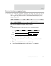
Parm Description Min Max Units Modes Notes
Table 475: SPI timing parameters


