PCI bus arbiter
428
NS9750 Hardware Reference
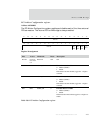
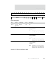
PCI Configuration 0 register
Address: A030 0010
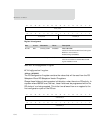
The PCI Configuration 0 register contains the values that will be read from the PCI
Device ID and PCI Vendor ID registers.
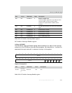
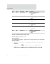
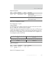
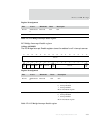
D06 R//W EN_BAR2 0 Enable bridge PCI Base Address register 2
0 Disable (default)
1 Enable
Note: Although
BAR_x can still be accessed
when
EN_BAR2 is 1, the address range
defined by
BAR_x will not be decoded.
D05 R/W EN_BAR1 0 Enable bridge PCI Base Address register 1
0 Disable (default)
1 Enable
Note: Although BAR_x can still be accessed
when
EN_BAR1 is 1, the address range
defined by
BAR_x will not be decoded.
D04 R/W EN_BAR0 0 Enable bridge PCI Base Address register 0
0 Disable (default)
1 Enable
Note: Although
BAR_x can still be accessed
when
EN_BAR0 is 1, the address range
defined by
BAR_x will not be decoded.
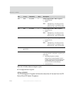
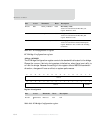
D03:01
Read only;
hard-wired to
0
Reserved N/A N/A
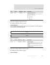
D00 R/W INTA2PCI 0 The inverted value of this bit drives the INTA#
output pin. INTA# is configured as a pseudo-open
drain output.
0 INTA# high impedance (default)
INTA# must be in high impedance state for
CardBus applications and for PCI applications
when NS9750 is the host, and provides the
interrupt controller for PCI interrupts.
1 Assert INTA# low
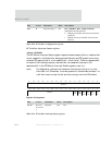
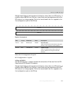
Bits Access Mnemonic Reset Description
Table 263: PCI Miscellaneous Support register


