www.digiembedded.com
663
Serial Control Module: SPI
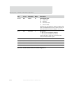
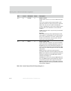
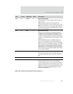
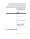
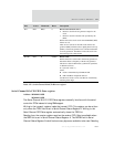
D22 R/W RXCINV 0 Receive clock invert
Controls the relationship between receive clock and
receive data:
When set to 0, the receive data input is sampled at
the rising edge transition of the receive clock. Use 0
for SPI modes 0 and 3.
When set to 1, the receive data input is sampled at
the falling edge transition of the receive clock. Use 1
for SPI modes 1 and 2.
D21 R/W SPCPOL 0/1 SPI transmit polarity
0 Idle high operation; use this value for SPI modes 1
and 3
1 Idle low operation; use this value for SPI modes 0 and
2
Defines the idle polarity of the SPI transmit clock.
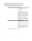
D20:19 R/W TDCR 00 Transmit clock divide rate
00 1x clock mode (only NRZ or NRZI allowed)
01 8x clock mode
10 16x clock mode
11 32x clock mode
Determines the divide ratio for the transmitter clock.
If the DPLL is not used, use the 1x clock mode value (00).
When DPLL is used in the application, selecting TDCR/
RDCR is a function of the transmitter encoding. The NRZ
and NRZI modes can use the 1x configuration; all other
encoding must use 8x, 16x, or 32x configuration mode.
The 8x configuration provides the highest possible data
rate; the 32x mode provides the highest possible
resolution.
The TMODE bit in this register is maintained for
NET+Arm family backward compatibility. When setting
the TDCR or RDCR register to a non-zero value, the
TMODE bit must be set to 1. When TMODE, TDCR, and
RDCR are all set to 0, the port defaults to 16x mode of
operation.
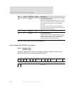
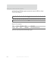
Bits Access Mnemonic Reset Description
Table 387: Serial Channel B/A/C/D Bit-rate register


