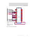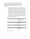
Pinout and signal descriptions
34
NS9750 Hardware Reference
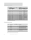
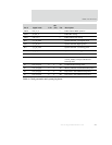
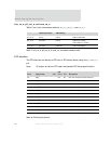
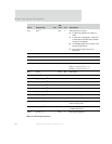
GPIO MUX
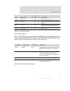
The BBus utility contains the control pins for each GPIO MUX bit. Each pin
can be selected individually; that is, you can select any option (00, 01, 02,
03) for any pin, by setting the appropriate bit in the appropriate register.
Some signals are muxed to two different GPIO pins, to maximize the number
of possible applications. These duplicate signals are marked as such in the
Descriptions column in the table. Selecting the primary GPIO pin and the
duplicate GPIO pin for the same function is not recommended. If both the
primary GPIO pin and the duplicate GPIO pin are programmed for the same
function, however, the primary GPIO pin has precedence and will be used.
The 00 option for the serial ports (B, A, C, and D) is configured for UART and
SPI mode, respectively; that is, the UART option is shown first, followed by
the SPI option if there is one. If only one value appears, it is the UART
value. SPI options all begin with SPI.
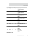
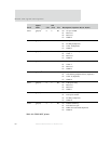
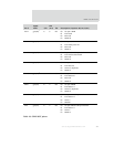
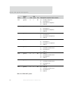
Pin #
Signal
name
U/D
OD
(mA)
I/O Description (4 options: 00, 01, 02, 03)
AF19 gpio[0]
1
U 2 I/O 00 Ser port B TxData / SPI port B dout
01 DMA ch 1 done (duplicate)
02 Timer 1 (duplicate)
03 GPIO 0
AE18 gpio[1] U 2 I/O 00 Ser port B RxData / SPI port B din
01 DMA ch 1 req (duplicate)
02 Ext IRQ 0
03 GPIO 1
AF18 gpio[2]
1
U 2 I/O 00 Ser port B RTS
01 Timer 0
02 DMA ch 2 read enable
03 GPIO 2
AD17 gpio[3] U 2 I/O 00 Ser port B CTS
01 1284 nACK (peripheral-driven)
02 DMA ch 1 req
03 GPIO 3
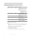
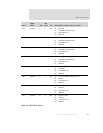
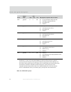
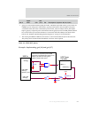
Table 10: GPIO MUX pinout


