


System control processor (CP15) registers
64
NS9750 Hardware Reference
R6: Fault Address register
Register R6 accesses the Fault Address register (FAR). The Fault Address register
contains the modified virtual address of the access attempted when a data abort
occurred. This register is updated only for data aborts, not for prefetch aborts; it is
updated also for alignment faults and external aborts that occur while the MMU is
disabled.
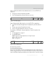
Use these instructions to access the Fault Address register:
MRC p15, 0, Rd, c6, c0, 0 ; read FAR
MCR p15, 0, Rd, c6, c0, 0 ; write FAR
Writing R6 sets the Fault Address register to the value of the data written. This is
useful for debugging, to restore the value of a Fault Address register to a previous
state.
The
CRm and opcode_2 fields SHOULD BE ZERO when reading or writing R6.
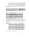
R7: Cache Operations register
Register R7 controls the caches and write buffer. The function of each cache
operation is selected by the
opcode_2 and CRm fields in the MCR instruction that writes
to CP15 R7. Writing other
opcode_2 or CRm values is UNPREDICTABLE.
Reading from R7 is UNPREDICTABLE, with the exception of the two test and clean
operations (see Table 27, “R7: Cache operations,” on page 66 and "Test and clean
operations" on page 67).
Use this instruction to write to the Cache Operations register:
MCR p15, opcode_1, Rd, CRn, CRm, opcode_2
Table 26 describes the cache functions provided by register R7. Table 27 lists the
cache operation functions and associated data and instruction formats for R7.
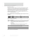
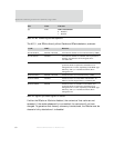
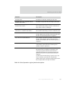
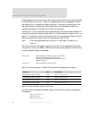
Lowest External abort Section page
0b1000
0b1010
Valid
Valid
Priority Source Size Status Domain
Table 25: Fault Status register status field encoding