www.digiembedded.com
655
Serial Control Module: SPI
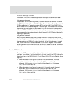
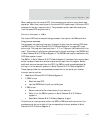
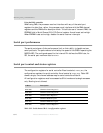
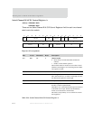
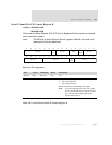
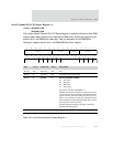
Serial Channel B/A/C/D Control Register B
Address: 9020 0004 / 0044
9030 0004 / 0044
There are two Serial Channel B/A/C/D Control Registers B within each two-channel
serial controller module.
Note:
The CE field in Serial Channel Control register A should not be set until
these control bits are stabilized.
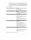
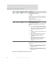
Register bit assignment
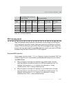
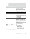
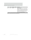
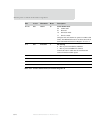
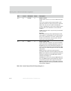
Bits Access Mnemonic Reset Description
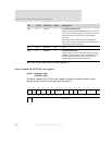
D31:26 R/W Reserved N/A N/A
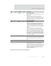
D25 R/W CSPOL 0 SPI chip select polarity
0 Active low chip select
1 Active high chip select
Defines the polarity of the SPI chip select signal.
Note: If you are using SPI slave mode, only a value
of 0 is valid; the SPI slave is fixed to an active
low chip select. Both values apply to SPI
master mode, however.
D24:22 R/W Not used 0 Must be written as 0.
Table 385: Serial Channel B/A/C/D Control Register B
Reserved
13121110987654321015 14
31 29 28 27 26 25 24 23 22 21 20 19 18 17 1630
MODE Not used
BIT
ORDR
Not used
CS
POL
Not used
Not
used
Reserved
Reserved


