Pinout and signal descriptions
44
NS9750 Hardware Reference
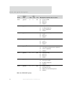
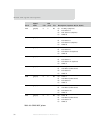
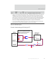
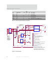
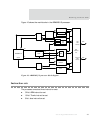
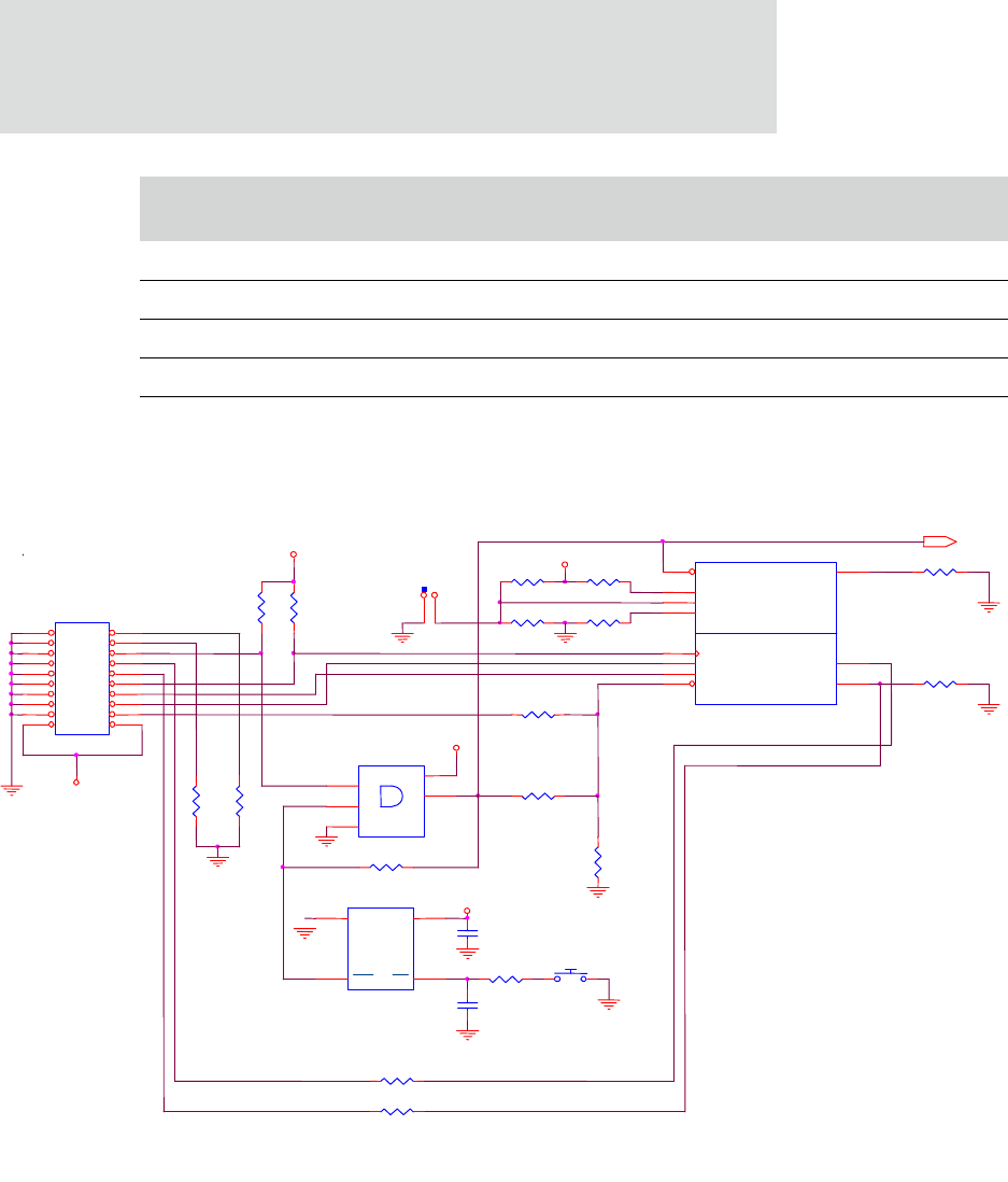
Figure 9: JTAG interface
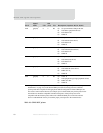
AE19 tdo 2 O Test data out
AC18 tms U I Test mode select
AF20 trst_n U I Test mode reset
AD19 rtck U 2 I/O Returned test clock, ARM core only
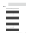
Bits Signal name U/D
OD
(mA)
I/O Description
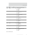
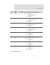
Table 14: JTAG interface/boundary scan pinout
TRSTn
R15 0
**
**
R4
33
R13
10K
PD_PIN19
TCK
**
3.3V
3.3V
RTCK
##
TDI
U2
NC7SZ08_SOT23
1
2
3
5
4
A
B
GND
VCC
Y
RSTn
JSRST
R9 2.4K
##
R7 10K
RESET monitor
Trip = 2.97V
R14
10K
JP1
R10 2.4K
R3
1.0K
##
JTDO
C3
.1
R2
10K
R16
0
R12
2.4K
JTAG 20
PIN
HEADER..
##
R5
33
TMS
3.3V
PD_PIN17
P1
HEADER 10X2.1SP
12
34
56
78
910
1112
1314
1516
1718
1920
R17
2.4K
SW1
SW_PB
SYSTEM CONTROL
JTAG
NS9750_BGA352
H25 AC21
AE20
AD18
AC18
AE19
AF20 AD19
AF21
AD20
AE21
RESET* RESET_DONE
TCK
TDI
TMS
TDO
TRST* RTCK
PLLTEST*
BISTEN*
SCANEN*
R6 10K
Should be
positioned on
PCB with pin 1
facing toward
board edge.
R8
2.4K
3.3V
RESETn
RESETn
JRTCK
U3
MAX811S_SOT143
1
2
4
3
GND
RST
+V
MR
**
R11 0
##
MRn
**
nTRST
TDO
**
C1
.001
R1
2.4K
JP1 recommended
instead of R9
during development
3.3V
phase,
NS9750
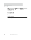
Notes
R8
out: Boot from flash/ROM/S_CS1n
in: Boot from SDRAM/CS0n using SPI_B
EEPROM on GPIO pins
R12
out: Internal PCI arbiter
in: External PCI arbiter bus
Debug
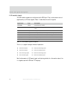
Load all except JP1/R9, R15, R16; R8 and R12
depend on board options
Disable blank or unprogrammed boot memory
Production with debug possibility
Omit parts with **
Production without debug possibility
Omit parts with ** and ##, as well as parts with **
When halting the CPU in debug mode, the
JSRST line must be pulsed low only one time.


