SPI-EEPROM boot logic
488
NS9750 Hardware Reference
SDRAM boot algorithm
Note:
The SDRAM boot logic communicates only with serial channel B.
These steps describe the SDRAM boot algorithm:
1 Pins boot_cfg[1:0] are both strapped high.
Power-on reset is deasserted.
The CPU is held in reset by the SPI-EEPROM boot module.
Serial channel B comes out of reset in SPI master mode.
2 A SPI-EEPROM read command at address zero is written to the Fifo Data register.
This is followed by seven more NOP entries.
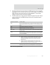
3 The RXFDB and RRDY fields are monitored in Status Register A. Only complete
words are read from the Fifo Data register. This process is repeated until four
words have been received. An internal word counter tracks how many words
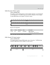
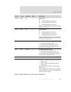
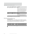
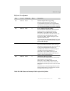
have been taken from the SPI-EEPROM (see Table 294, “Boot algorithm actions,”
on page 489 for information about any actions taken).
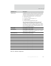
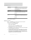
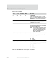
DynamicConfig0 Field B (buffer enable, in the DynamicConfig0 register) should be set
to 0 (buffers disabled). The buffers will be enabled by hardware as
part of the boot process.
See your ARM documentation.
DynamicRasCas0 See the Memory Controller chapter.
Reserved The remaining bytes are undefined. The final byte address of header
is one of the following, depending on the pad entry length:
0x7F
0x80
0x81
Boot code Must immediately follow the configuration header. The first byte
address of the boot code is one of the following, depending on the pad
entry length:
0x80
0x81
0x82
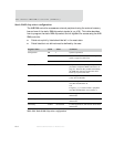
EEPROM entry Description
Table 293: ARM boot configuration


