Dynamic memory controller
162
NS9750 Hardware Reference
Dynamic memory controller
Write protection
Each dynamic memory chip select can be configured for write-protection by setting
the appropriate bit in the write protect (P) field on the Dynamic Memory
Configuration register (see "Dynamic Memory Configuration 0–3 registers" on page
225). If a write access is performed to a write-protected memory bank, an ERROR
response is generated on the
HRESP[1:0] signal.
Access sequencing and memory width
The data width of each chip select must be configured by programming the
appropriate Dynamic Memory Configuration register. When the chip select data bus
width is narrower than the transfer initiated from the current AMBA bus master, the
internal bus transfer takes several external bus transfers to complete. If chip select 4
is configured as 16-bit wide memory, for example, and a 32-bit read is initiated, the
AHB bus stalls while the memory controller reads two consecutive words from
memory. During these accesses, the memory controller block demultiplexes the two
16-bit words into one 32-bit word and places the result onto the AHB bus.
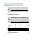
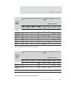
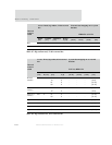
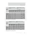
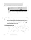
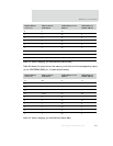
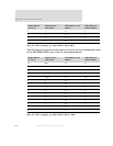
Byte 000 01 1011 - [23:16] - -
Byte 000 00 0111 [31:24] - - -
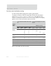
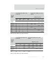
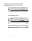
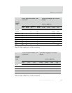
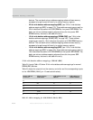
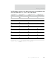
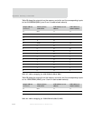
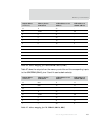
Access: Write, big endian, 32-bit
external bus
System data mapping on to external
databus
Internal
transfer
width
DATA
HSIZE
[2:0]
HADDR
[1:0]
BLSOUT
[3:0]
[31:24] [23:16] [15:8] [7:0]
Table 90: Big endian write, 32-bit external bus


