www.digiembedded.com
477
BBus Bridge
Peripheral DMA read access
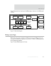
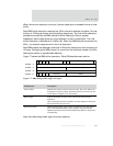
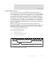
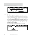
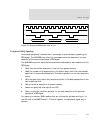
Figure 78 and Figure 79 show how the DMA engine performs read accesses of an
external peripheral. The
CLK signal shown is for reference, and its frequency is equal
to 1/2 the speed grade of the part. The rising edge of the
READ_EN signal coincident
with the assertion of the chip select signal must cause the peripheral to place the
next quantum of data on the bus. The width of the READ_EN signal is always equal to
one reference
CLK period. The delay from the falling edge of CS# to the rising edge of
ACK is always equal to one reference CLK period. The width of the CS# assertion is
defined in the Static Memory Read Delay register (see "Static Memory Read Delay 0–3
registers" on page 236).
DMA read accesses from an external peripheral are treated as asynchronous
operations by the NS9750. It is critical that the required width of the
CS# assertion be
computed correctly and programmed into the Static Memory Read Delay register.
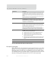
Total access time can be computed as shown:
Total access time = T
a
+ T
b
+ T
c
+ 10.0
The variables are defined as follows:
Figure 78: Peripheral DMA single read access
T
a
= Peripheral read access time
T
b
= Total board propagation including buffers
T
c
= One reference CLK cycle period
DATA VALID
READ_EN
DQ
CS#
CLK


