Pinout and signal descriptions
18
NS9750 Hardware Reference
Pinout and signal descriptions
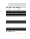
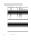
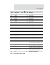
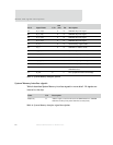
Each pinout table applies to a specific interface, and contains the following
information:
More detailed signal descriptions are provided for selected modules.
System Memory interface
Heading Description
Pin # Pin number assignment for a specific I/O signal
Signal Pin name for each I/O signal. Some signals have multiple function modes and are
identified accordingly. The mode is configured through firmware using one or more
configuration registers.
_n in the signal name indicates that this signal is active low.
U/D U or D indicates whether the pin is a pullup resistor or a pulldown resistor:
U — Pullup (input current source)
D — Pulldown (input current sink)
If no value appears, that pin is neither a pullup nor pulldown resistor.
I/O The type of signal: input, output, or input/output.
OD (mA) The output drive of an output buffer. NS9750 uses one of three drivers:
2 mA
4 mA
8 mA
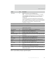
Pin # Signal Name U/D
OD
(mA) I/O Description
A21 addr[0] 8 O Address bus signal
B20 addr[1] 8 O Address bus signal
C19 addr[2] 8 O Address bus signal
A20 addr[3] 8 O Address bus signal
B19 addr[4] 8 O Address bus signal
Table 3: System Memory interface pinout


