


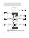

Caches and write buffer
108
NS9750 Hardware Reference
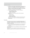
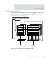
Table 46 gives the page table C and B bit settings for the DCache (R1: Control register
C bit = M bit = 1), and the associated behavior.
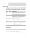
1 0 DCache enabled, MMU disabled. All data accesses are noncachable,
nonbufferable, with no protection checks. All addresses are flat-mapped; that
is, VA=MVA=PA.
1 1 DCache enabled, MMU enabled. All data accesses are cachable or
noncachable, depending on the page descriptor C bit and B bit (see Table 46:
"Page table C and B bit settings for DCache"), and protection checks are
performed. All addresses are remapped from VA to PA, depending on the
MMU page table entry; that is, the VA is translated to an MVA and the MVA
is remapped to a PA.
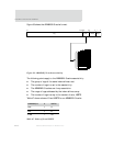
Page
table C
bit
Page
table B
bit
Description ARM926EJ-S behavior
0 0 Noncachable,
nonbufferable
DCache disabled. Read from external memory. Write as a
nonbuffered store(s) to external memory. DCache is not updated.
0 1 Noncachable,
bufferable
DCache disabled. Read from external memory. Write as a
buffered store(s) to external memory. DCache is not updated.
1 0 Write-through DCache enabled:
Read hit Read from DCache.
Read miss Linefill.
Write hit Write to the DCache, and buffered store to
external memory.
Write miss Buffered store to external memory.
1 1 Write-back DCache enabled:
Read hit Read from DCache.
Read miss Linefill.
Write hit Write to the DCache only.
Write miss Buffered store to external memory.
Table 46: Page table C and B bit settings for DCache
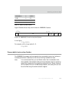
R1 C bit R1 M bit ARM926EJ-S behavior
Table 45: R1: Control register I and M bit settings for DCache