USB timing
832
NS9750 Hardware Reference
USB timing
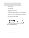
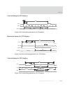
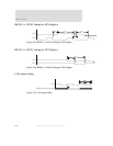
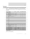
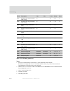
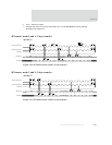
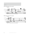
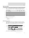
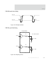
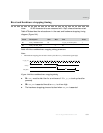
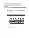
Table 477 and Table 478 describe the values shown in the USB timing diagrams
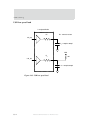
(Figure 141 through Figure 143).
Notes:
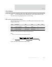
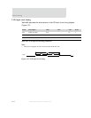
1 Load shown in Figure 142, "USB full speed load," on page 833.
2 U1/U2.
3 Includes resistance of 27 ohm ±2 ohm external series resistor.
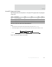
4 Load shown in Figure 143, "USB low speed load," on page 834.
5 Excluding the first transition from the idle state.
Parm Description Min Max Unit Notes
U1 Rise time (10% – 90%) 4 20 ns 1
U2 Fall time (10% – 90%) 4 20 ns 1
U3 Differential rise and fall time matching 90 111.11 % 2, 5
U4 Driver output resistance 28 44 ohms 3
Table 477: USB full speed timing parameters
Parm Description Min Max Unit Notes
U1 Rise time (10% – 90%) 75 300 ns 4
U2 Fall time (10% – 90%) 75 300 ns 4
U3 Differential rise and fall time matching 80 125 % 2, 5
Table 478: USB low speed timing parameters


