www.digiembedded.com
127
Memory Controller
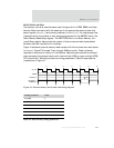
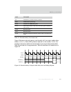
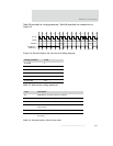
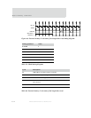
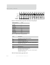
Figure 43 shows an external memory read transfer with two output enable delay
states (
WAI TO EN= 2). Seven AHB cycles are required for the transfer, five for the
standard read and an additional two because of the output delay states added.
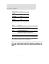
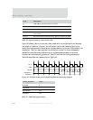
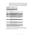
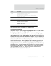
Table 53 provides the timing parameters. Table 54 describes the transactions for
Figure 43.
Figure 43: External memory 2 output enable delay state read timing diagram
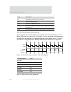
Cycle Description
T0 AHB address provided to memory controller.
T0-T1 AHB transaction processing.
T1-T4 Arbitration of AHB memory ports.
T4-T5 Static memory address, chip select, and control signals submitted to
static memory.
T5-T6 Read wait state 1.
T6-T7 Read wait state 2.
T7-T8 Read data returned from the static memory. Data is provided to the
AHB.
Table 52: External memory 2 wait state read
ADDR
DATAIN
STCSOUT_n
A
D(A)
COEOUT_n
clk_out
T0 T1 T2 T3 T4 T5 T6 T7 T8


