www.digiembedded.com
137
Memory Controller
deasserted a cycle before the chip select, at the end of the transfer. BLSOUT_n (byte
lane signal) has the same timing as
WEOUT_n (write enable signal) for writes to 8-bit
devices that use the byte lane selects instead of the write enables.
SRAM
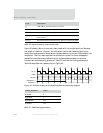
Write timing for SRAM starts with assertion of the appropriate memory bank chip
selects (STCSOUT[n]_n) and address signals (ADDROUT[27:0]_n). The write access time is
determined by the number of wait states programmed for the
WA IT WR field in the
Static Memory Write Delay register (see "Static Memory Write Delay 0–3 registers" on
page 238). The
WAI TTUR N field in the bank control register (see "Static Memory Turn
Round Delay 0–3 registers" on page 239) determines the number of bus turnaround
wait states added between external read and write transfers.
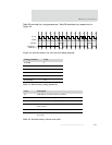
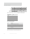
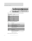
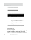
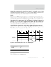
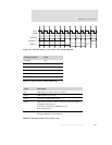
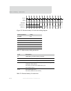
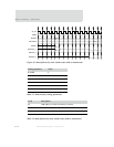
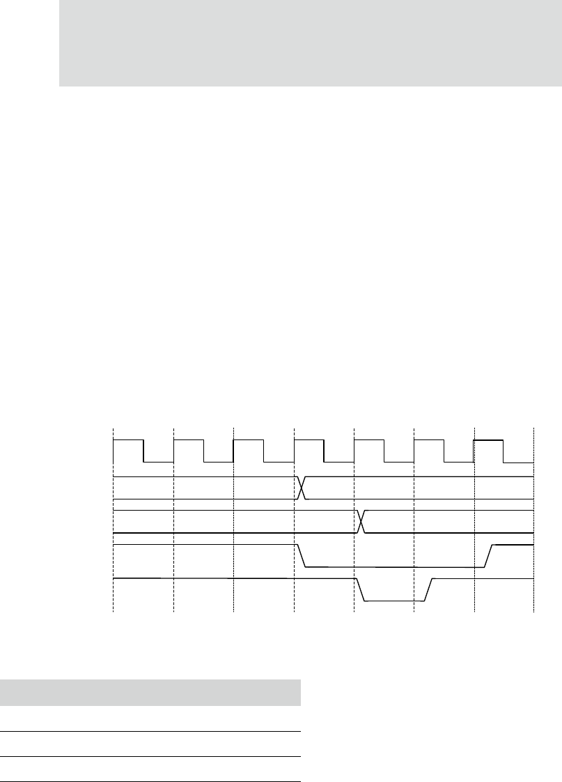
Figure 49 shows a single external memory write transfer with minimum zero wait
states (
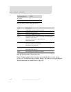
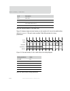
WA IT WR =0). One wait state is added. Table 65 provides the timing parameters.
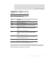
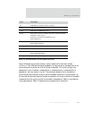
Table 66 describes the transactions for Figure 49.
Figure 49: External memory 0 wait state write timing diagram
Timing parameters Value
WAITRD N/A
WAITOEN N/A
WAITPAGE N/A
WAITWR 0
Table 65: Static memory timing parameters
ADDR
DATAOUT
STCSOUT_n
WOEOUT_n
A
D(A)
clk_out
T0 T1 T2 T3 T4 T5
T6


