


System control processor (CP15) registers
58
NS9750 Hardware Reference
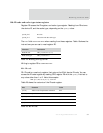
R1: Control register
Register R1 is the control register for the ARM926EJ-S processor. This register
specifies the configuration used to enable and disable the caches and MMU (memory
management unit). It is recommended that you access this register using a read-
modify-write sequence.
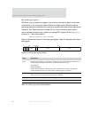
For both reading and writing, the
CRm and opcode_2 fields SHOULD BE ZERO. Use these
instructions to read and write this register:
MRC p15, 0, Rd, c1, c0, 0 ; read control register
MCR p15, Rd, c1, c0, 0 ; write control register
All defined control bits are set to zero on reset except the V bit and B bit.
The V bit is set to zero at reset if the VINITHI signal is low.
The B bit is set to zero at reset if the BIGENDINIT signal is low, and set to one
if the
BIGENDINIT signal is high.
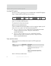
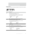
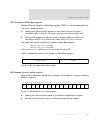
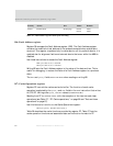
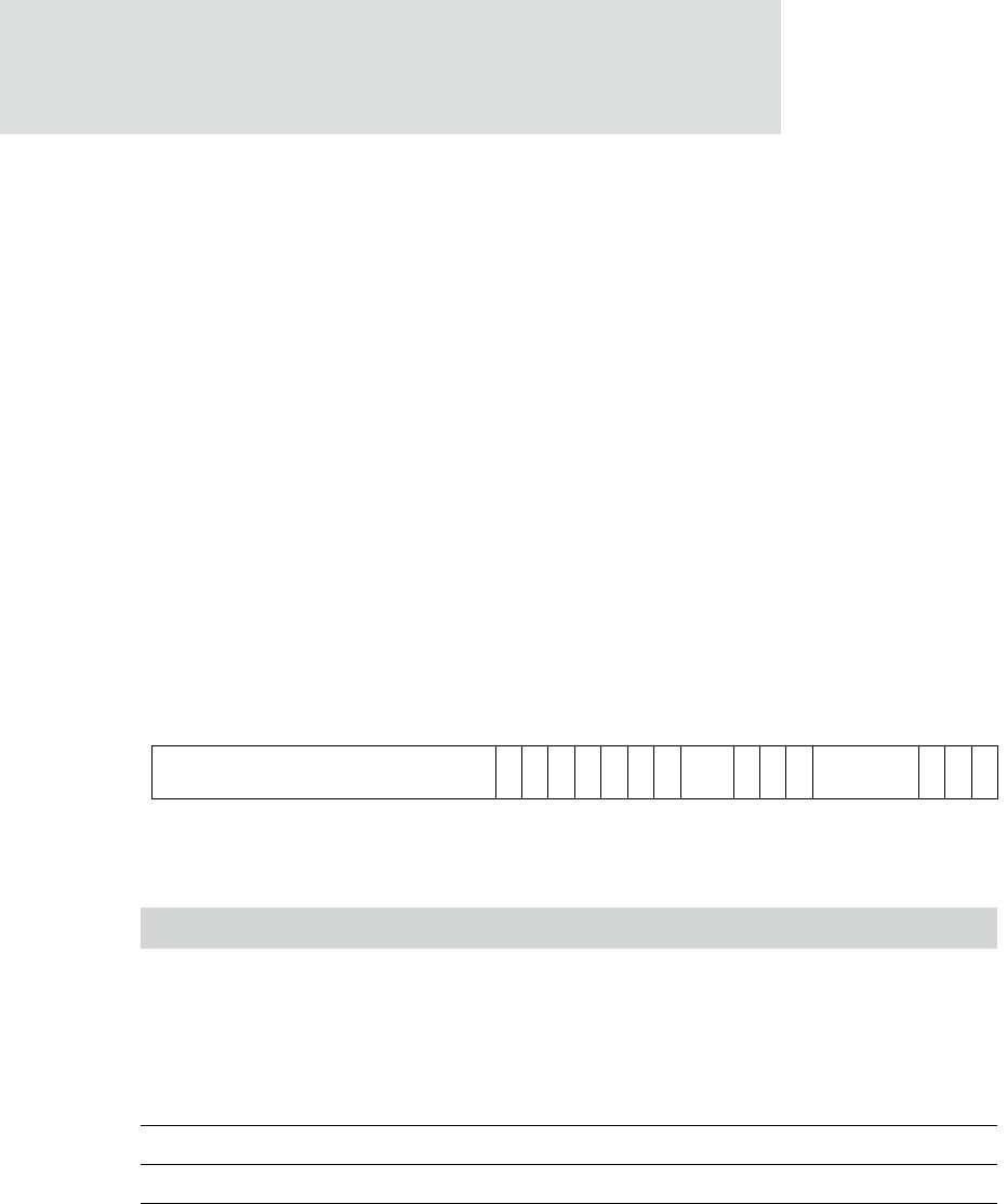
Figure 13 shows the Control register format. Table 22 describes the Control register
bit functionality.
Figure 13: Control register format
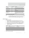
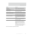
Bits Name Function
[31:19] N/A Reserved:
When read, returns an UNPREDICTABLE value.
When written, SHOULD BE ZERO, or a value read from bits
[31:19] on the same processor.
Use a read-modify-write sequence when modifying this
register to provide the greatest future compatibility.
[18] N/A Reserved, SBO. Read = 1, write =1.
[17] N/A Reserved, SBZ. read = 0, write = 0.
[16] N/A Reserved, SBO. Read = 1, write = 1.
Table 22: R1: Control register bit definition
131 19 16 15 12 11 10 9 8 7 3 0218 17 14 13 6
S
B
Z
SBZ
S
B
O
S
B
O
L
4
R
R
VI
SBZ
RSB
SBO
CAM