


Serial port control and status registers
662
NS9750 Hardware Reference
D26 R/W TXEXT 0 Drive transmit clock external
0 Disable
1 Enable
Enables the transmitter clock to be driven on GPIO pins
gpio[7], gpio[15], gpio[23], gpio[27] for serial ports B, A,
C, and D, respectively.
For SPI master mode, set to 1 to enable.
For SPI slave mode, set to 0 to disable.
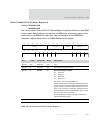
D25:24 R/W CLKMUX 00 Bit-rate generator clock source
Controls the bit-rate generator clock source. The bit-rate
generator can be configured to use one of four clock
sources:
00
x1_sys_osc/M (see Table 380, “Bit-rate generation
clock sources,” on page 645 for more information).
This selection is not valid when the PLLBP field in
the PLL Configuration register is set to 1.
01 BCLK
This is the recommended setting for SPI master and
slave operation.
10 Input clock defined by external receive clock on
GPIO pins gpio[6], gpio[14], gpio[22], and
gpio[26] for serial ports B, A, C, and D,
respectively.
11 Input clock defined by external transmit clock on
GPIO pins gpio[7], gpio[15], gpio[23], and
gpio[27] for serial ports B, A, C, and D,
respectively.
D23 R/W TXCINV 0 Transmit clock invert
Controls the relationship between transmit clock and
transmit data:
When set to 0, transmit data changes relative to the
falling edge transition of the transmit clock. Use 0
for SPI modes 0 and 3.
When set to 1, transmit data changes relative to the
rising edge transition of the transmit clock. Use 1 for
SPI modes 1 and 2.
Bits Access Mnemonic Reset Description
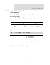
Table 387: Serial Channel B/A/C/D Bit-rate register