www.digiembedded.com
295
System Control Module
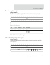
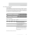
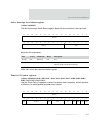
Reset and Sleep Control register
Address: A090 0180
The Reset and Sleep Control register resets each module on the AHB bus. To use sleep
mode, the CPU must reset and stop the clocks to all modules not used to wake up the
CPU. The memory controller must be reset and then re-enabled. The code that resets
the memory controller must be loaded into instruction cache first. The last step is to
set the CSE bit (D19) in the Reset and Sleep Control register.
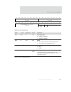
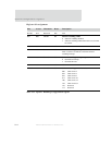
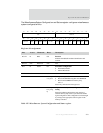
Register bit assignment
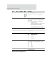
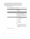
Bits Access Mnemonic Reset Definition
D31:22 N/A Reserved N/A N/A
D21 R/W BBW 0x0 BBus aggregate interrupt wakeup enable
0 Do not wake up on a BBus aggregate interrupt.
1 Wake up on a BBus aggregate interrupt.
D20 R/W I2CW 0x0 I2C interrupt wake up enable
0 Do not wake up on an I2C interrupt.
1 Wake up on an I2C interrupt.
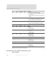
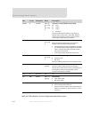
D19 R/W CSE 0x0 CPU sleep enable
System software writes a 1 to this bit to reset and stop the
clock to the CPU. Note that software is responsible for
stopping the clocks to all other modules before setting this
bit.
This bit must be cleared after the CPU is woken up, before
reentering the sleep state.
Table 186: Reset and Sleep Control register
13121110987654321015 14
31 29 28 27 26 25 24 23 22 21 20 19 18 17 1630
Reserved
Reserved
LCDC MEMC RsvdBBT PCIM MACM
Not
used
I2CW CSE SMWE EWE PI3WEBBW


