www.digiembedded.com
473
BBus Bridge
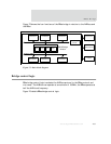
Cycles and BBus arbitration
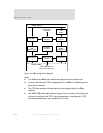
During a normal cycle, each bus master cycle is allowed only one read/write cycle if
another bus master is waiting. There are two exceptions to this rule: burst
transactions and read-modify-write transactions.
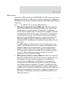
In a burst transaction, the master can perform more than one read or write cycle. In
a read-modify-write transaction, the bus master performs one read and write cycle to
the same location.
BBus peripheral address map (decoding)
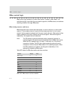
The BBus address map is divided to allow access to the internal modules and external
resources routed through the internal peripherals. The BBus configuration registers
are located at base address 0xA040 0000 and are dedicated a 1 MB address space. The
BBus peripherals are located at base address
0x9000 0000 and span a 256 MB address
space. Each BBus peripheral, with the exception of the SER port controllers, resides
in a separate 1 MB address space.
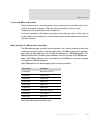
Table 288 specifies the address space given to each peripheral.
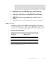
Base address Peripheral
0x9000 0000 BBus DMA controller
0x9010 0000 USB controller
0x9020 0000 SER Port #B
0x9020 0040 SER Port #A
0x9030 0000 SER Port #C
0x9030 0040 SER Port #D
0x9040 0000 IEEE-1284 controller
0x9050 0000 I2C controller
0x9060 0000 BBus utility
Table 288: BBus peripheral address map


