www.digiembedded.com
665
Serial Control Module: SPI
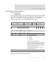
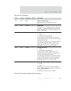
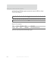
Serial Channel B/A/C/D FIFO Data register
Address: 9020 0010 / 0050
9030 0010 / 0050
The Serial Channel B/A/C/D FIFO Data registers manually interface with the serial
controller FIFOs instead of using DMA support.
Writing to the transmit register loads the transmit FIFO. This register can be written
only when the TRDY field is set in Serial Channel Status Register A. Writing to the
Serial Channel FIFO Data register automatically clears the TRDY bit.
Reading from the receive register empties the receive FIFO. Data is available when
the RRDY bit is set in Serial Channel Status Register A. The RXFDB field in Serial
Channel Status Register A identifies how many bytes are available to be read. Reading
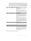
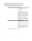
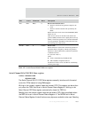
D15 R/W RICS 0 Receive internal clock source
0 Receiver uses the bit-rate generator output for the
clock.
1 Receiver uses the extracted clock provided by the
DPLL.
Defines the receive clock source when the RXSRC (D29)
field is set to 0.
There are two sources for internal clocks: the bit-rate
generator (BRG) and the receiver digital phase lock loop
(DPLL). The bit-rate generator uses a divider mechanism
for clock generation. The DPLL extracts the clock from
the incoming receive data stream.
D14:00 R/W N 0x0000 Divisor value
Defines the divisor value used in the bit-rate generator to
determine effective frequency of the bit-rate generator.
The divisor value for SPI master (synchronous operation)
is defined as follows:
N = ((F
CLK
/2 * DR) - 1)
where:
FCLK = Determined by CLKMUX field
DR = DataRate = Required data rate
For SPI slave mode, N is not used. Bit rate is defined by
incoming clock edges.
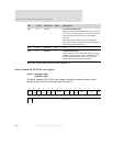
Bits Access Mnemonic Reset Description
Table 387: Serial Channel B/A/C/D Bit-rate register


