www.digiembedded.com
303
System Control Module
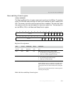
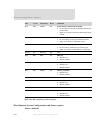
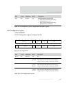
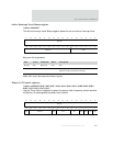
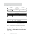
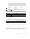
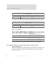
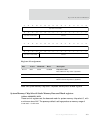
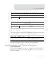
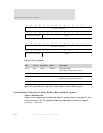
System Memory Chip Select 0 Dynamic Memory Base and Mask registers
Address: A090 01D0 / 01D4
These control registers set the base and mask for system memory chip select 1, with
a minimum size of 4K. The powerup default settings produce a memory range of
0x0000 0000 — 0x0FFF FFFF.
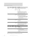
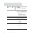
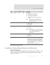
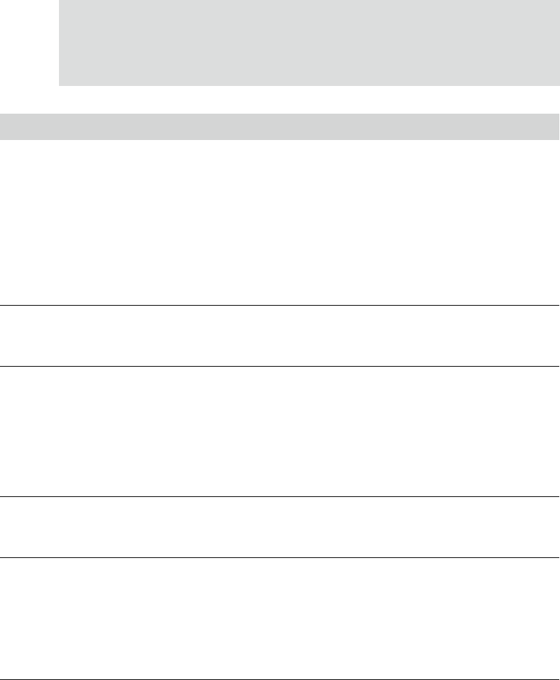
D05:04 R/W TM 0x0 Timer mode
00 Internal timer or external event
01 External low-level, gated timer
10 External high-level, gated timer
11 Concatenate the lower timer. Not applicable on
timer 0.
Note: When either external gated timer option is
selected, the timer clock select bits (08:06)
determine the frequency.
D03 R/W INTS 0x0 Interrupt select
0 Interrupt disable
1 Generate IRQ
D02 R/W UDS 0x0 Up/down select
0 Up counter
1 Down counter
Note: When configured as an up counter, the terminal
count is 0xFFFF_FFFF. When configured as a
down counter, the terminal count is
0x0000_0000.
D01 R/W TSZ 0x0 32- or 16-bit timer
0 16-bit timer
1 32-bit timer
D00 R/W REN 0x0 Reload enable
0 Halt at terminal count. The timer must be disabled,
then enabled to reload the timer when the terminal
count is reached. The interrupt select (INTS) bit must
be cleared during the interrupt service routine when
this mode is selected.
1 Reload and resume count at terminal count.
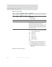
Bits Access Mnemonic Reset Description
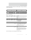
Table 190: Timer Control register


