www.digiembedded.com
131
Memory Controller
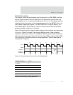
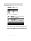
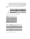
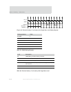
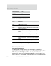
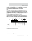
Figure 46 shows a burst of two wait state reads with the length specified. The WA IT RD
value is used for all transfers in the burst. Table 59 provides the timing parameters.
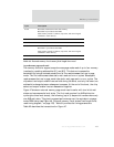
Table 60 describes the transactions for Figure 46.
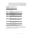
WAITWEN N/A
WAITTURN N/A
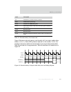
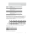
Cycle Description
T0 AHB address provided to memory controller.
T0-T1 AHB transaction processing.
T1-T4 Arbitration of AHB memory ports.
T4-T5 Static memory read 0 address, chip select, and control signals
submitted to static memory.
T5-T6 Static memory read 1 address, chip select, and control signals
submitted to static memory. Read data 0 returned from static
memory.
Read data 0 is provided to the AHB.
T6-T7 Static memory read 2 address, chip select, and control signals
submitted to static memory. read data 1 returned from the static
memory.
Read data 1 is provided to the AHB.
T7-T8 Static emory read 3 address, chip select, and control signals submitted
to static memory. Read data 2 returned from the static memory.
Read data 2 is provided to the AHB.
T8-T9 Read data 3 returned from the static memory.
Read data 3 is provided to the AHB.
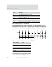
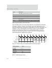
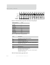
Table 58: External memory zero wait fixed length burst read
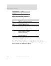
Timing parameter Value
Table 57: SRAM timing parameters


