www.digiembedded.com
143
Memory Controller
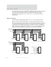
Flash memory
Write timing for flash memory is the same as for SRAM devices.
Bus turnaround
The memory controller can be configured for each memory bank to use external bus
turnaround cycles between read and write memory accesses. The
WAI TTUR N field can
be programmed for 1 to 16 turnaround wait states, to avoid bus contention on the
external memory databus. Bus turnaround cycles are generated between external bus
transfers as follows:
Read to read (different memory banks
Read to write (same memory bank)
Read to write (different memory banks)
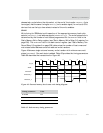
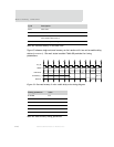
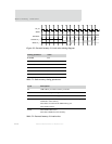
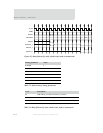
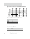
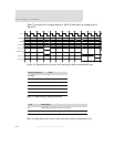
Figure 53 shows a zero wait read followed by a zero wait write with default
turnaround between the transfers of two cycles because of the timing of the AHB
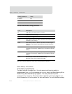
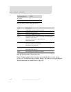
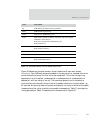
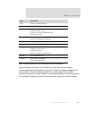
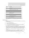
transfers. Table 73 provides the timing parameters. Table 74 describes the
transactions for Figure 53.
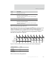
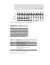
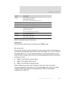
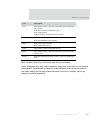
T6-T7 Static memory writes data 0.
Write enable taken inactive.
Write data 1 is read from AHB memory port.
T7-T8 Static memory control signals taken inactive.
T8-T9 Memory controller processing.
T9-T10 Static memory transfer 1, address, chip select, and control signals
submitted to static memory.
Write enable inactive.
Write data submitted to static memory.
T10-T11 Write enable taken active.
T11-T12 Static memory writes data 1.
Write enable taken inactive.
Cycle Description
Table 72: External memory 2 0 wait writes


