www.digiembedded.com
53
Working with the CPU
Note:
In all cases, reading from or writing any data values to any CP15 registers,
including those fields specified as
UNPREDICTABLE, SHOULD BE ONE, or
SHOULD BE ZERO, does not cause any physical damage to the chip.
Register summary
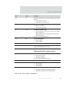
CP15 uses 16 registers.
Register locations 0, 5, and 13 each provide access to more than one
register. The register accessed depends on the value of the
opcode_2 field in
the CP15
MRC/MCR instructions (see "Accessing CP15 registers" on page 52).
Register location 9 provides access to more than one register. The register
accessed depends on the value of the
CRm field (see "Accessing CP15
registers" on page 52).
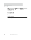
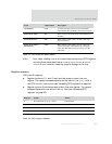
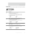
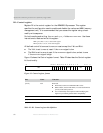
UNDEFINED UND An instruction that accesses CP15 in the manner
indicated takes the UNDEFINED instruction exception.
SHOULD BE ZERO SBZ When writing to this field, all bits of the field SHOULD
BE ZERO
.
SHOULD BE ONE SBO When writing to this location, all bits in this field
SHOULD BE ONE.
SHOULD BE ZERO or
PRESERVED
SBZP When writing to this location, all bits of this field
SHOULD BE ZERO or PRESERVED by writing the
same value that has been read previously from the
same field.
Term Abbreviation Description
Table 17: CP15 terms and abbreviations
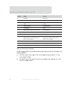
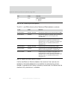
Register Reads Writes
0 ID code (based on
opcode_2 value) Unpredictable
0 Cache type (based on opcode_2 value) Unpredictable
1 Control Control
2 Translation table base Translation table base
3 Domain access control Domain access control
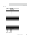
Table 18: CP15 register summary


