www.digiembedded.com
273
System Control Module
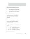
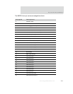
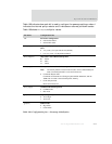
Table 168 indicates how each bit is used to configure the powerup settings, where 1
indicates the internal pullup resistor and 0 indicates an external pulldown resistor.
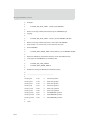
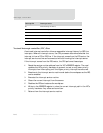
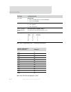
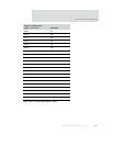
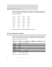
Table 169 shows
PLL ND[4:0] multiplier values.
Pin name Configuration bits
rtck PCI arbiter configuration
0 External PCI arbiter
1 Internal PCI arbiter
boot_strap[0] Chip select 1 byte_lane_enable_n/write_enable_n configuration bootstrap
select
0
write_enable_n for byte-wide devices (default)
1 byte_lane_enable_n (2.4K pulldown added)
boot_strap[4:3] Chip select 1 data width bootstrap select
00 16 bits
01 8 bits
11 32 bits
boot_strap[2] Memory interface read mode bootstrap select
Note: An external pulldown resistor must be used to select command delayed
mode. Clock delayed mode is reserved for future use.
0 Command delayed mode
Commands are launched on a 90-degree phase-shifted AHB clock, and the
AHB clock is routed to the external dynamic memory.
1 Clock delayed mode
Reserved for future use.
boot_strap[1] CardBus mode bootstrap select
0 CardBus mode
1 PCI mode
gpio[49] Chip select polarity
0 Active high
1 Active low
gpio[44] Endian mode
0 Big endian
1 Little endian
Table 168: Configuration pins — Bootstrap initialization


