www.digiembedded.com
811
Timing
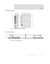
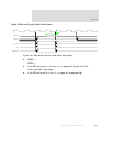
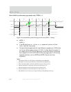
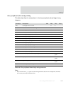
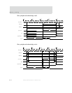
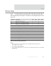
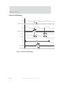
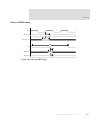
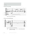
Slow peripheral acknowledge timing
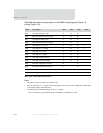
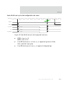
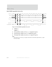
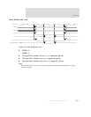
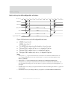
This table describes the values shown in the slow peripheral acknowledge timing
diagrams.
Table 469: Slow peripheral acknowledge timing parameters
Note:
1 Only one of the four st_cs_n signals is used. The diagrams show the active low configuration, which can
be reversed (active high) with the PC field.
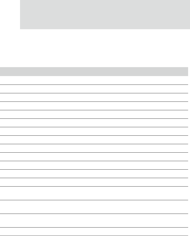
Parameter Description Min Max Unit Notes
M15 clock high to data out valid +2 ns
M16 data out hold time from clock high -2 ns
M17 clock high to address valid +2 ns
M18 address hold time from clock high -2 ns
M19 clock high to st_cs_n low +2 ns 1
M20 clock high to st_cs_n high +2 ns 1
M21 clock high to we_n low +2 ns
M22 clock high to we_n high +2 ns
M23 clock high to byte_lanes low +2 ns
M24 clock high to byte_lanes high +2 ns
M26 data input hold time to rising clk 4.5 ns
M27 clock high to oe_n low +2 ns
M28 clock high to oe_n high +2 ns
M29 address/chip select valid to ta_strb high 2 CPU
cycles
M30 ta_strb pulse width 4 8 CPU
cycles
M31 ta_strb rising to chip select/address change 4 10 CPU
cycles
M32 data setup to ta_strb rising 0 ns


