


DEFINITY Enterprise Communications Server Release 6
Maintenance for R6vs/si
555-230-127
Issue 1
August 1997
Maintenance Object Repair Procedures
Page 10-946PI-BD (Processor Interface Circuit Pack)
10
PI-BD (Processor Interface Circuit
Pack)
The TN765 Processor Interface (PI) circuit pack provides a front-end processor
to the TN777 Processor circuit pack. The PI circuit pack implements the packet
layer and link layer of the X.25 protocol (DCS, AUDIX, CMS, OCM links) as well
as the link layer of the ISDN-PRI protocol (ISDN links). A system without high or
critical reliability supports up to two circuit packs. A high or critical reliability
system supports up to four Processor Interface circuit packs, two in each carrier.
Only one pair of the circuit packs on a single carrier can be active at a given
time. The other two are in Standby mode. The TN765 is a downloadable circuit
pack. This means that at reboot, system power-up, or via system technician
command, Processor Interface firmware is downloaded to the circuit pack. For
other restarts, a Checksum Test is performed on the firmware. If the Checksum
Test fails, then the firmware is downloaded again. The firmware can be
automatically downloaded at any time using the reset interface PCS system
technician command.
On the Active SPE complex or in an unduplicated system, Processor Interface
maintenance is used for alarming the circuit pack. If System Communication
Interface (PI-SCI) finds an error or alarm condition that can be associated with an
on-board problem with the Processor Interface (PI-BD) circuit pack, then it
alarms both the System Communication Interface and the Processor Interface
circuit pack. Processor Interface circuit pack maintenance is also used to test the
common circuit pack functions on the circuit pack. If these tests fail, a circuit
pack level alarm is raised on the Processor Interface circuit pack (PI-BD). Port
level alarms are raised against PI-PT. See PI-PT (Processor Interface Port)
Maintenance documentation for details.
On the Standby SPE complex, the testing of the Processor Interface circuit pack
is different. The Standby Processor Interface circuit pack is tested daily via
scheduled maintenance or on system technician demand. These tests are to
check the Standby PIs hardware and firmware so that if an SPE interchange
takes place, the Processor Interface communication links (DCS, ISDN, or AUDIX,
for example) recover on the new Active Processor Interface circuit pack in a
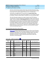
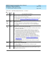
1. Where P is the port network number (1 for PPN only); C is the carrier designation (for example,
A or B for processor complex circuit packs); and S is the address of the slot in the carrier where
the circuit pack is located (for example, 1 or 2 for either the first or second Processor Interface
circuit packs).
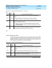
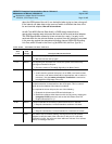
MO Name (in
Alarm Log)
Alarm
Level Initial Command to Run
1
Full Name of MO
PI-BD MINOR test interface PCS sh Processor Interface Circuit Pack
PI-BD
WARNING
test interface PCS sh Processor Interface Circuit Pack